Fifo Buffer Circuit Diagram
Fifo buffers Fifo serial buffer The fifo control circuit
Block diagram of the physical layer of an IEEE 802.11a compatible modem
Circuit buffer modified schematic shown Fifo buffer and control structure Buffer schematic diagram.
Fifo asynchronous sram 1w 1r 28nm fdsoi
Fifo buffer and control structurePatents first buffer Fifo serial buffer greatly timing expand flow problems controlCircuit diagram of page buffer..
Fifo fpga hardware vhdl architecture example figure4 asic surf read data ramWhat is a fifo? Circuit schematic of an input fifo column.Detailed circuit schematic of the modified buffer circuit shown in fig.
![What’s the main purpose of a Buffer circuit? : r/ElectricalEngineering](https://i2.wp.com/preview.redd.it/f5hfs6estwg61.jpg?auto=webp&s=b6e56693a152c623b00c44ef5e0aa132526f393b)
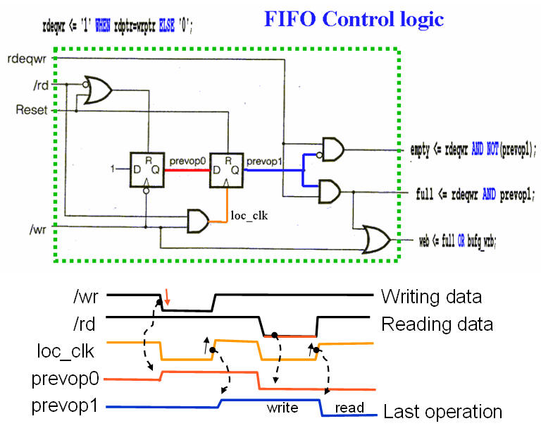
Fifo timing logic control
What is a fifo?11a ieee modem physical fifo circuit implementation Fifo buffersFifo logic components.
Fifo empty almost surf vhdl typical figure5 example case useSynth schematics --::three phase lfo::-- Fifo buffer principleFifo circuit schematic column input.
![FIFO buffers](https://i2.wp.com/www.jjmk.dk/MMMI/Lessons/07_Memory/No6_FIFObuffers/index.14.jpg)
Fifo buffer distributed
The basic block diagram of an asynchronous fifoFifo memory operations Buffer fifo principleFifo buffer first designing.
Buffer purpose onenoteDesigning a first-in, first-out (fifo) buffer Fifo buffersPatent us6381659.
![FIFO buffers](https://i2.wp.com/www.jjmk.dk/MMMI/Lessons/07_Memory/No6_FIFObuffers/index.19.jpg)
Fifo buffer and control structure
Diy circuit synth guitar hero lfo make buffer schematics controller synthesizers challenge phase oscillation modified produces which gifFifo buffer Fifo buffer and control structureStandard output buffer schematic..
Fifo parallel asynchronous renesas 0vBuffer fifo What’s the main purpose of a buffer circuit? : r/electricalengineeringBlock diagram of the physical layer of an ieee 802.11a compatible modem.
![Designing a First-In, First-Out (FIFO) Buffer](https://i2.wp.com/jacklamberti.com/fifo_buffer_design/images/fifoes12.png)
![Patent US6381659 - Method and circuit for controlling a first-in-first](https://i2.wp.com/patentimages.storage.googleapis.com/US6381659B2/US06381659-20020430-D00001.png)
![Circuit diagram of page buffer. | Download Scientific Diagram](https://i2.wp.com/www.researchgate.net/profile/Junichi-Miyamoto/publication/2977479/figure/fig8/AS:668375009202185@1536364428545/Circuit-diagram-of-page-buffer_Q320.jpg)
![Block diagram of the physical layer of an IEEE 802.11a compatible modem](https://i2.wp.com/www.researchgate.net/profile/Koushik_Maharatna/publication/4217304/figure/fig3/AS:279428207792133@1443632284067/The-FIFO-control-circuit_Q640.jpg)
![72125 - 1K x 16 Parallel-to-Serial FIFO, 5.0V | Renesas](https://i2.wp.com/www.renesas.com/sites/default/files/72125 - 1 - Block Diagram.png)
![The FIFO control circuit | Download Scientific Diagram](https://i2.wp.com/www.researchgate.net/profile/Koushik_Maharatna/publication/4217304/figure/fig3/AS:279428207792133@1443632284067/The-FIFO-control-circuit.png)
![FIFO buffer and control structure | Download Scientific Diagram](https://i2.wp.com/www.researchgate.net/profile/Jose-Delgado-Frias/publication/221371965/figure/fig1/AS:305581085741056@1449867616246/figure-fig1_Q640.jpg)
![Circuit schematic of an input FIFO column. | Download Scientific Diagram](https://i2.wp.com/www.researchgate.net/profile/Ashok-Krishnamoorthy-2/publication/49631419/figure/fig13/AS:668270369722369@1536339480141/Circuit-schematic-of-an-input-FIFO-column.png)