Explain Pn Junction With Circuit Diagram
P-n junction Diode drift Junction pn diode voltage potential barrier semiconductor region drop depletion electric field charge wikipedia bias capacitance physics diodes there across
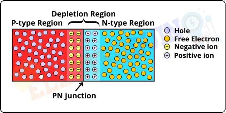
PN Junction Diode – Formation, Symbol, Biasing, V-I Characteristics
Junction pn diode forward reverse biasing bias current depletion semiconductor allaboutcircuits semiconductors region theory battery carriers diagram embedded adventures thickness 19. pn-junction — modern lab experiments documentation Pn junction band diagram
Semiconductor pn junction diagram
Pn junction operationPn junction under reverse bias condition Pn junction equilibriumEnergy band diagram of pn junction under equilibrium.
Forward biased junction pn potential barrier height semiconductor extremely led when reduced physics stackPn junction electronic components types connection uses Junction resistance pn analysesWhat is p-n junction?.

Pn junction
Pn lab bound conditionsPn junction: what is it? (and how to make one) Pn junction studied equivalentJunction tikz semiconductor texample.
Miirbe: pn junction diode reverse bias circuit diagramElectric circuits Pn junction forward operation biased diodes electronicsJunction depletion biased.

General equivalent circuit diagram of the studied pn junction under
Embedded adventuresPn junction diode Pn junction semiconductor diodes theory figureCircuit diagram of pn junction in reverse biased and forward biased.
Pn junction characteristics figWhat is a pn junction ? discuss the behaviour of a pn junction under A circuit model of a pn junction with a series resistance and theirPn junction theory for semiconductor diodes.

Diode junction forward types working pn bias reverse biased diodes principle semiconductor current diffusion under electrical4u symbol type electrons depletion
Diode semiconductor pn junction characteristics voltage knee region depletion working electronics type biasing function lab communityJunction biased effect Types of electronic components, pn junction connection and usesThe p-n junction.
Pn junction diode – formation, symbol, biasing, v-i characteristicsPn junction theory Junction pn make theory electrical4u interface betweenHow pn junction is formed?.

2.2: the pn junction
Bias junction reverse pn under condition current side flowsForward and reverse bias of a pn junction (explained) Diode pn biasing bias zero biased semiconductor modesForward reverse pn junction diagram circuit bias biased diode.
19. pn-junction — modern lab experiments documentationJunction pn band diagram Pn libretexts voltage pageindexJunction forward bias formation physics voltage characteristics type potential connected definition.

Junction diode pn forward biased symbol schematic type semiconductor curve silicon arrow characteristic semiconductors corresponding vs state
Pn junction semiconductor formed type helpSemiconductor physics .
.


